During the 2008/2009 Spring semester I worked at the Research Institute for Technical Physics and Materials Science of the Hungarian Academy of Sciences in Budapest, focusing on graphene’s transport characteristics, especially on its direction dependence, with Peter Neumann.
Graphene itself is peculiar material – the one atom thick layer of carbon atom was thought to be unstable until its discovery in 2004. Since then researchers are trying to discover the possibilities that materials like graphene can contribute to modern technology.
So far it has been proven that its electron mobility can be far better than that of copper or other conducting materials (15000 cm2/Vs !) , depending on the doping profile, which would enable us to build ballistic transistors, with better amplification and higher maximum operating frequencies.
The other interesting phenomenon about graphene is that because of its hexagonal structure, besides electrons Dirac-fermions appear and relativistic effects can be observed but “relatively” slowly: with only the speed of light / 300.
Graphene is a zero-gap semiconductor, meaning that the conductance and the valence band meet in only one point, where they travel all with the same speed: the Fermi speed. This could also be exploited in the future.
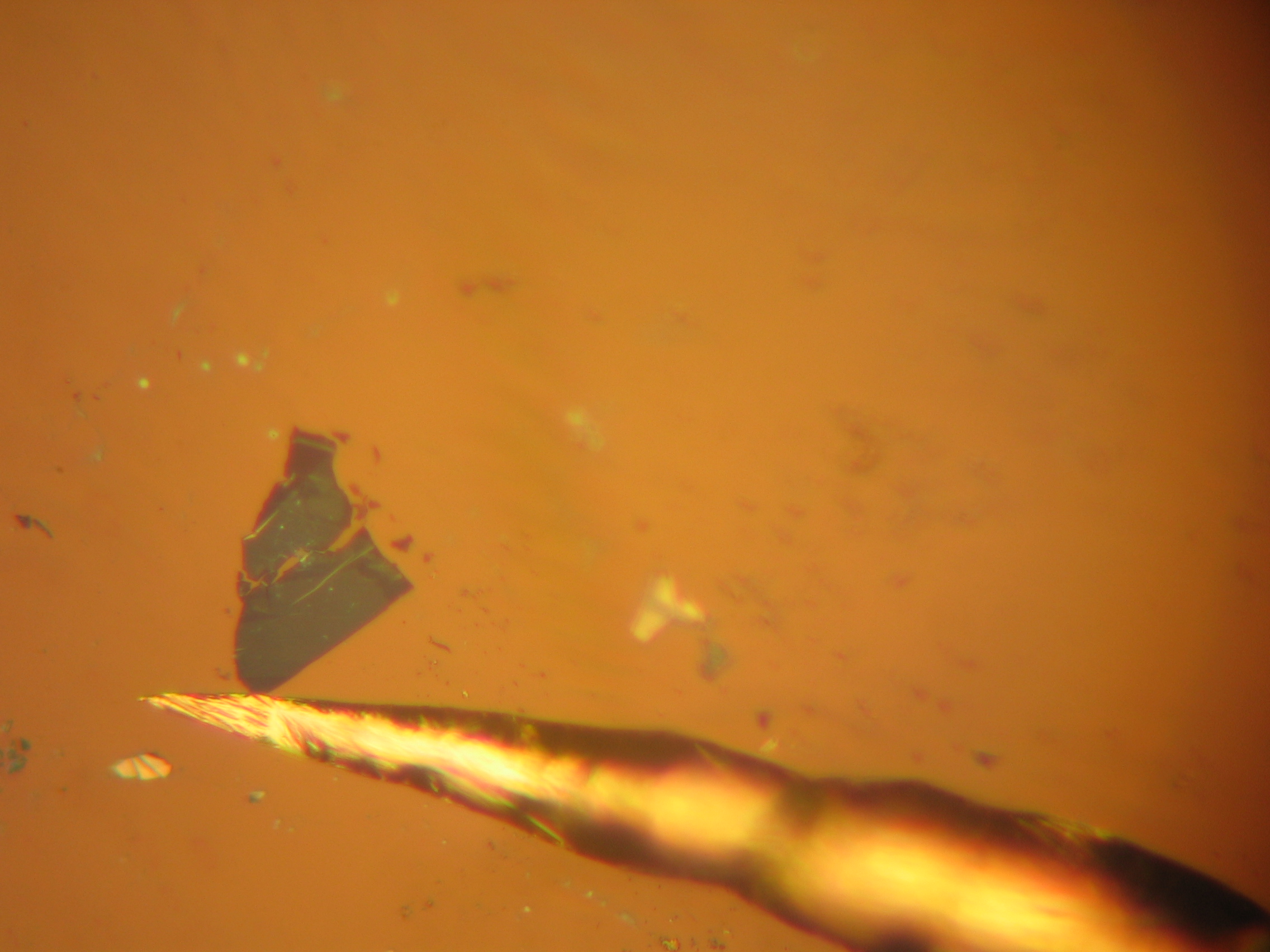
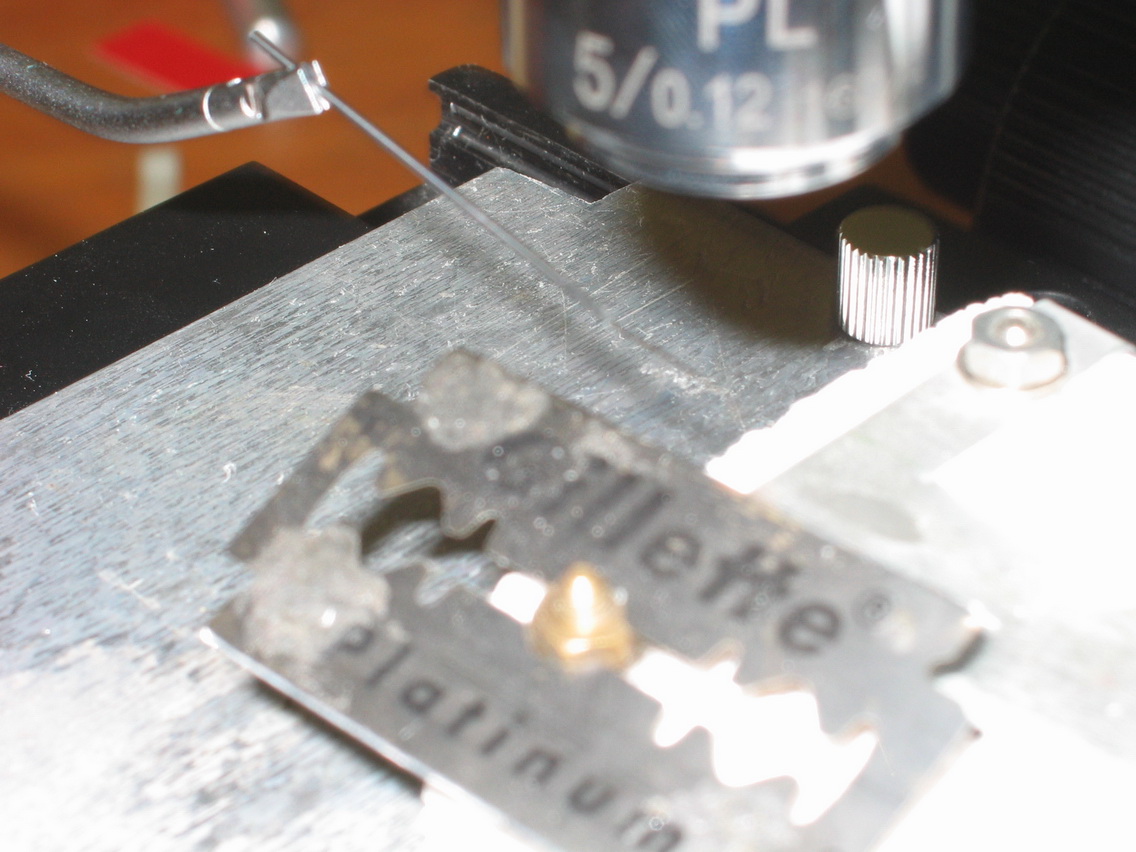
The first stage of my research was to “produce” graphene. I followed the steps developed by the research group led by Dr. K. Novoselov, in Manchester: they used mechanical exfoliation to extract graphene from HOPG (Highly Oriented Pyrolytic Graphite).
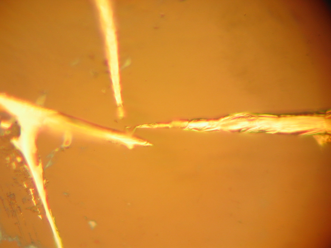
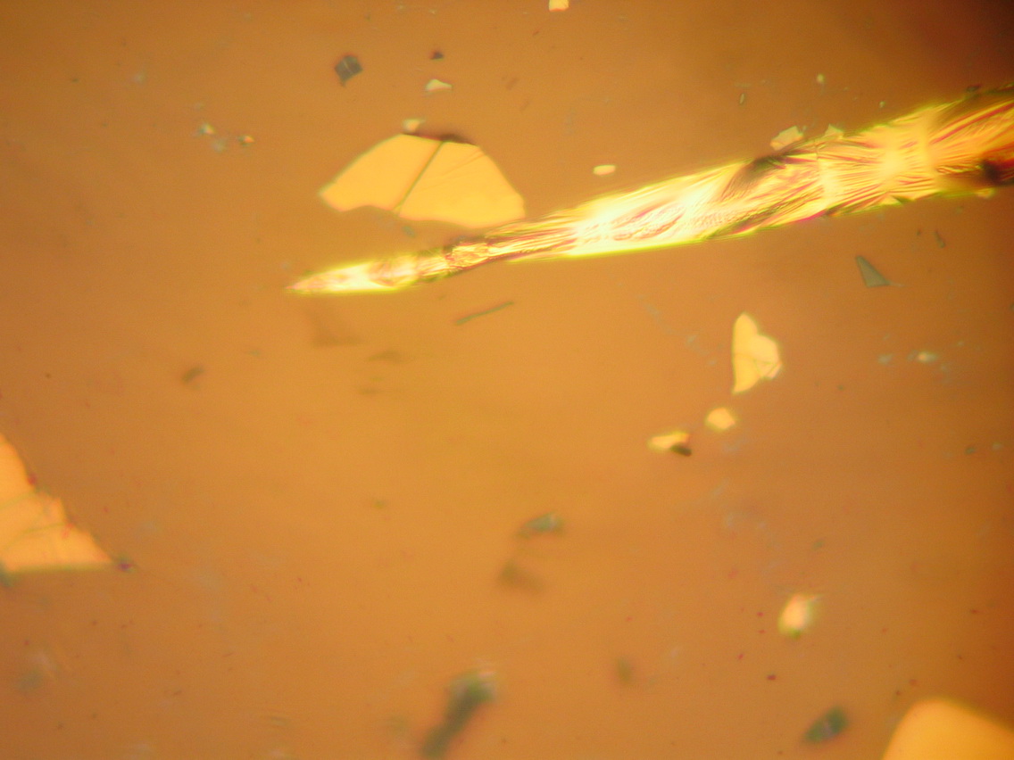
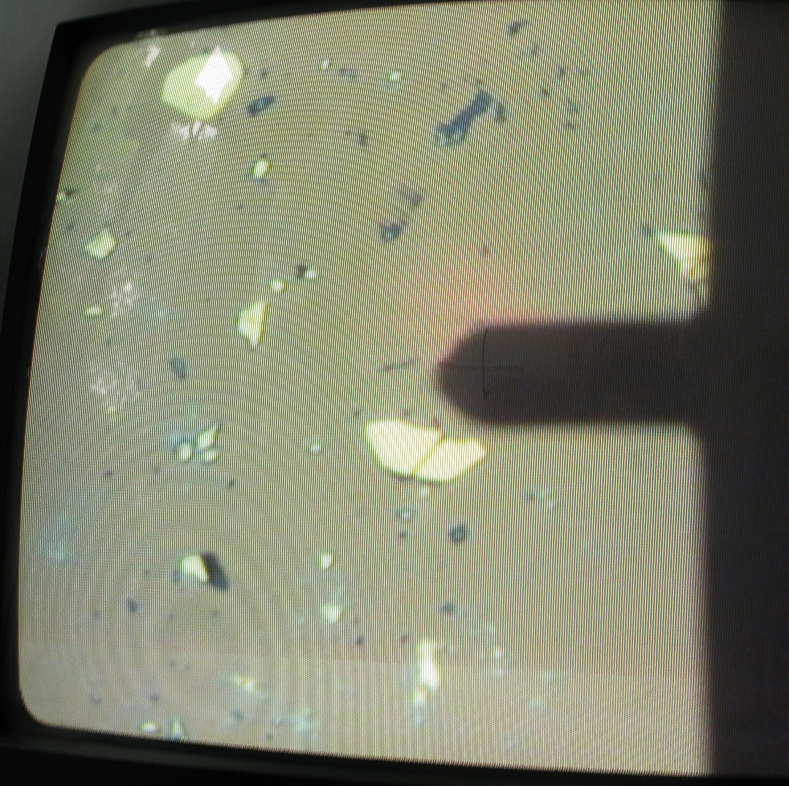
Basically, the whole trick in the procedure lies in the odd interference that can be observed when placing graphene and graphite on a specific width of SiO2. Novoselov discovered that on a 90 nm width of oxide, the 3.35 ?? wide graphene and the n * 3.35 ?? (where n is the number of layers in the graphite) can be distinguished even under an optical microscope: the different number of layers appear in different colors.
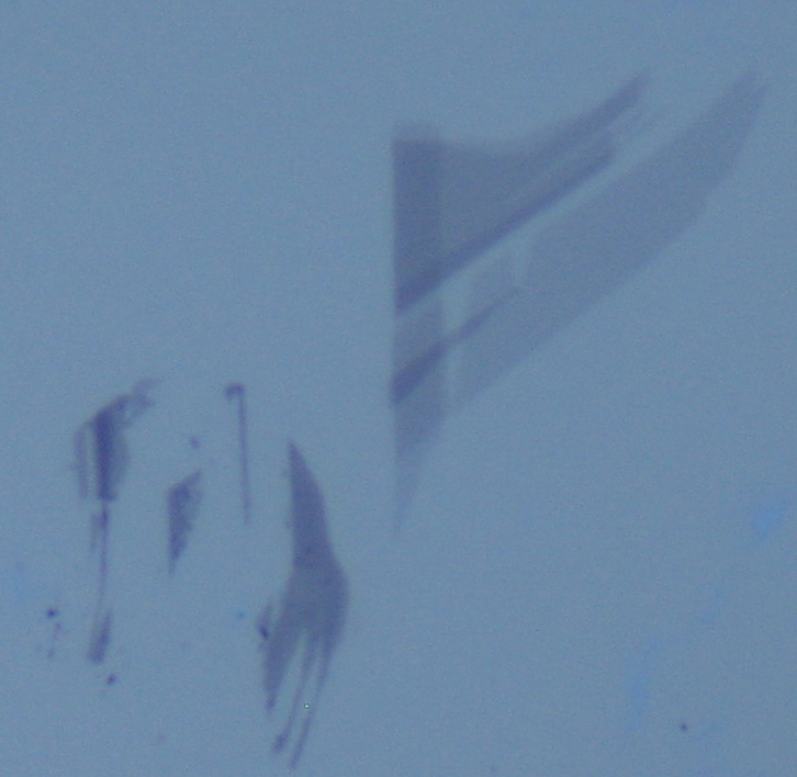
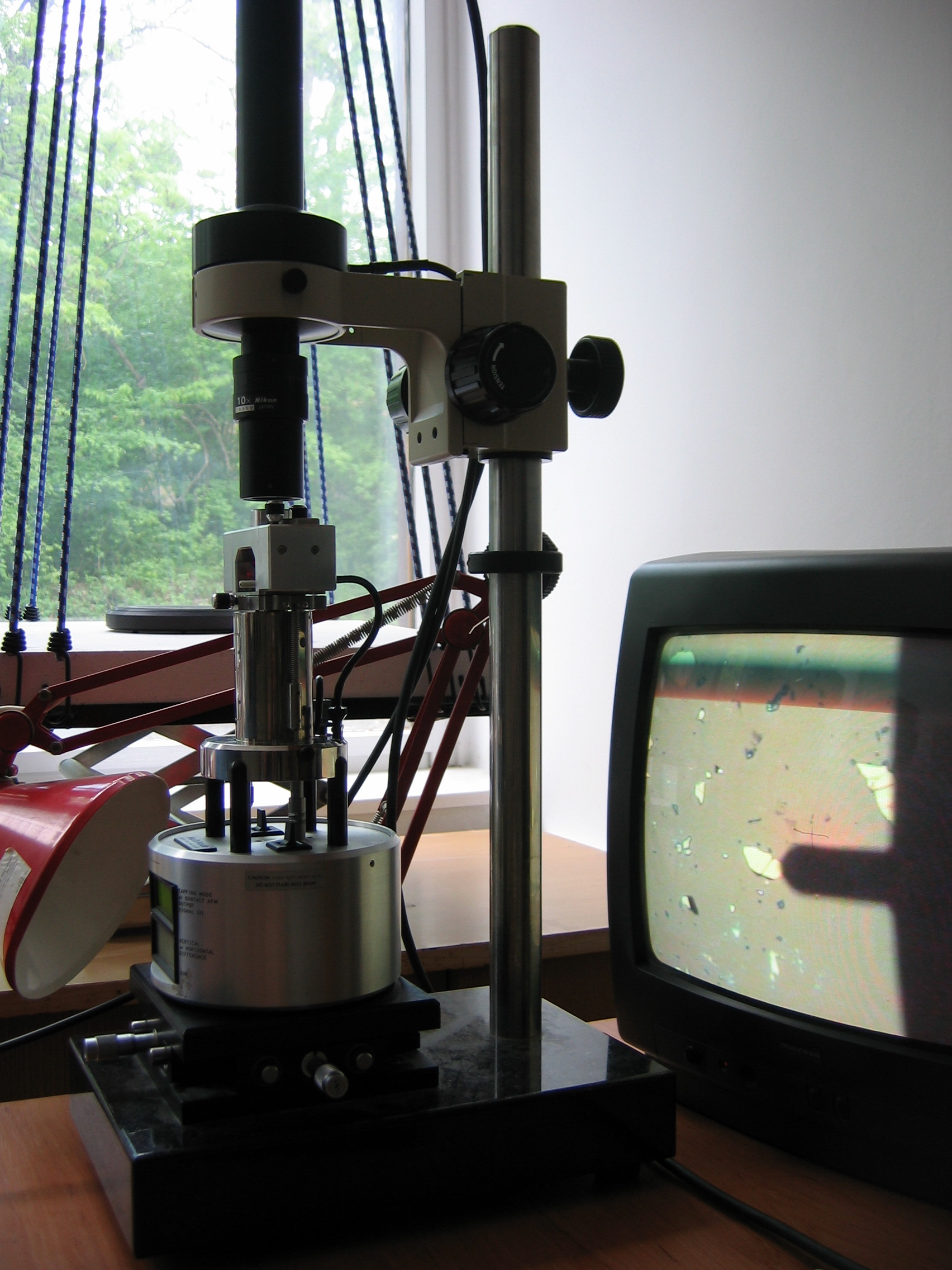
I used the same trick. and after I marked several “wannabe-graphenes” on my sample, I observed it under AFM, selecting those structures, which proved to be graphene after all.
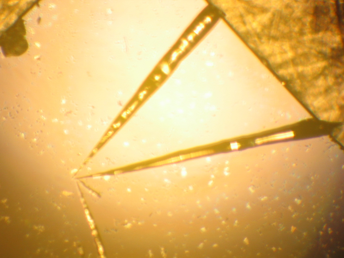
After I knew where my sample contained graphene, I was ready to contact the found nanostructures: I used In wires, with nano-manipulators, which allowed me to contact my structure to a source-meter, which did the measurement of the structure’s transport characteristics.
The results were surprising: in some cases graphene appeared to be semi-conducting, and in some conducting. The reason for semiconducting properties is being investigated at the present.