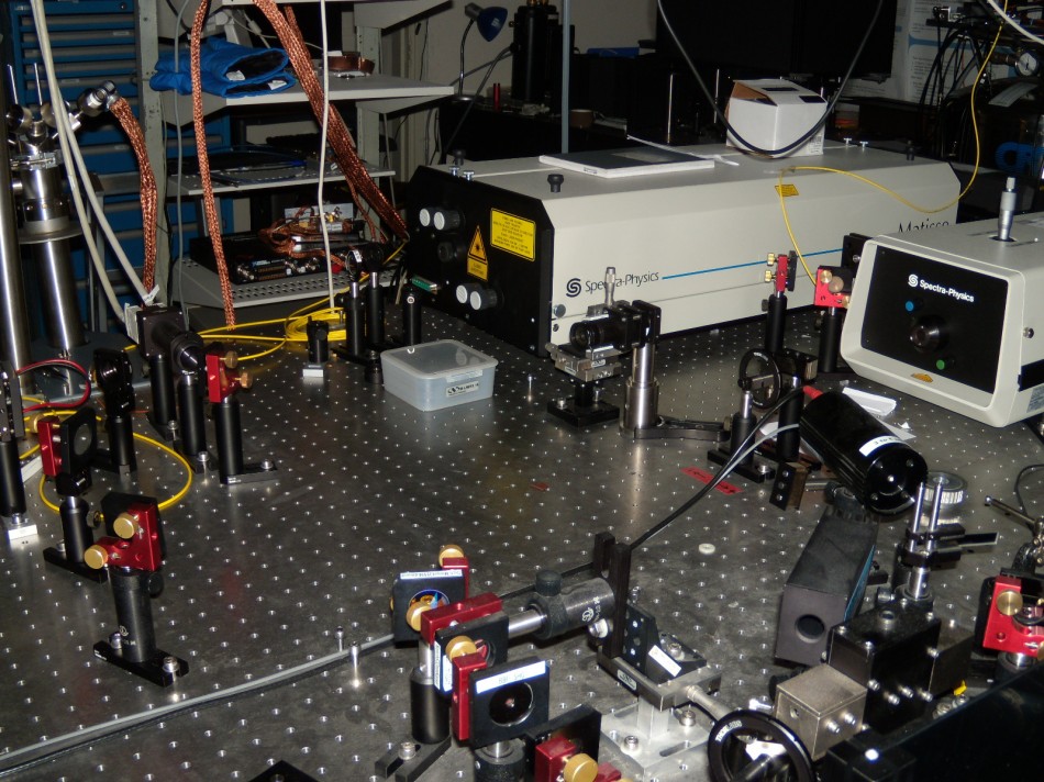
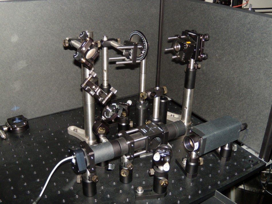
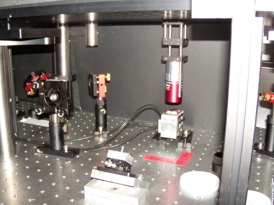
For the last 6 months, I have been underground in a lab of the Kavli Institute of Nanosciences in Delft, the Netherlands. During this time with my supervisor, Gilles Buchs, we constructed an optical setup in order to investigate future device possibilities emerging from the peculiar optical properties of carbon nanotubes.
The era of microelectronics is approaching its end because scaling down electronic device dimensions is slowly reaching fundamental physical limits. In order to continue the envisioned path of Gordon E. Moore – who predicted that the computational power of semiconductor electronics will double, roughly every two years – new technology has to be implemented. Nanotechnology provides a new perspective in fabrication, in comparison with the usual top-down scheme used in microelectronics, with the so-called bottom-up technique where nanostructures are assembled at nearly atomic levels. Working according to this philosophy, device dimensions can be scaled down to individual atoms.
The phenomena occurring at the nanometer scale cannot be described by classical physics anymore, but only by quantum mechanics. When the dimensions of objects shrink down to the nanometer scale, new properties emerge. One well-known example for this is given by graphite.
Graphite (a stacking of two-dimensional, sp2-bonded carbon layers) is known as a mechanically soft material, which is used in pencil leads. Now, if one imagines isolating a small sheet of a graphite monolayer (graphene) and rolling it into a cylinder with a nanometric diameter, one will obtain a nano-object with amazing mechanical (tensile strength 80 times higher than high strength steel), thermal (better than copper) and electronic properties (completely described by tube geometry). Such objects called carbon nanotubes (CNT) have been discovered in 1991 by Sumio Iijima at NEC and since then have led to an explosion of research activities in many labs worldwide. Furthermore, recent studies showed very promising optical properties which allow new applications and research in nanotube-based optoelectronics. Their importance even grew in the recent past, since in the eld of quantum information processing, carbon nanotubes are potential candidates that are able to naturally link solid-state qubits used for information processing (such as single spins), with flying qubits used to transmit quantum information (photons).
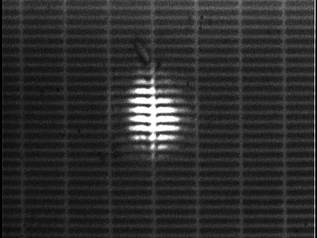
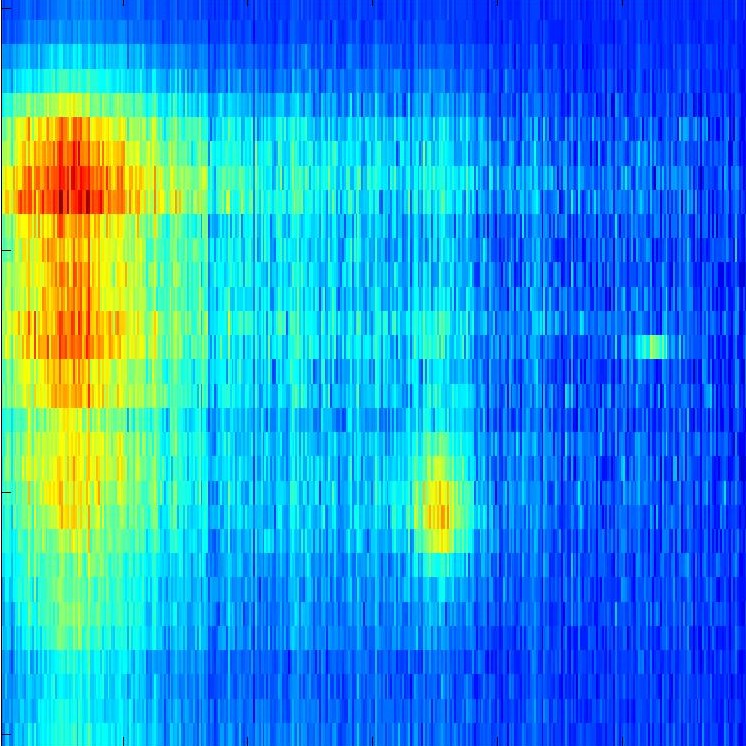
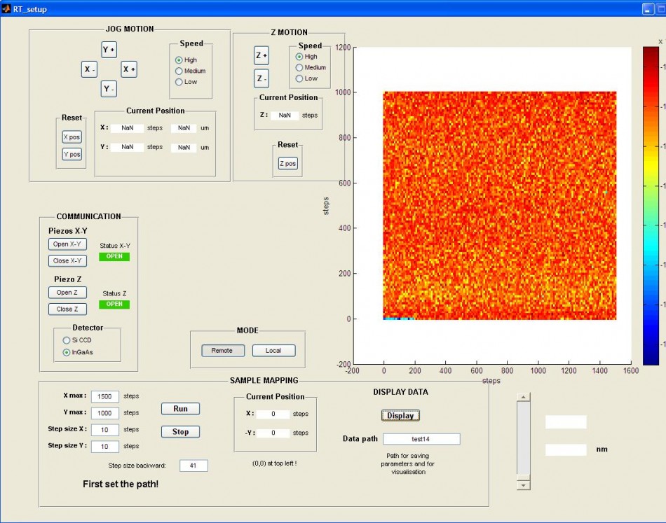
The goal of my thesis is to get familiarized with carbon nanotube physics and related experimental techniques. Here the focus was put on the optical properties of single-wall carbon nanotubes (SWCNT). I studied the photoluminescence (PL) of suspended carbon nanotubes on diverse samples. I implemented a system to facilitate the investigation of the photoluminescence excitation (PLE) mapping, which helped identify the structure of the investigated nanotubes. Furthermore, I have come across an effect called bleaching, which corresponds to the decay of the PL signal. Based on the available literature, we addressed the reasons behind this observation.
